Or gate using 2 NANDS [closed]
 https://stackoverflow.com/questions/1304300
-
19-09-2019 - |
 italiano
 english
 français
 española
 中国
中国 日本の
日本の العربية
 Deutsch
 한국어
한국어 Português
 Russian
Question
The diagrams I've seen for making an OR gate from a NAND gate use 3 NAND gates but if you have both inputs connected to both connectors of a NAND gate and then the output of this gate as inputs to both connectors of a second NAND gate it should behave like an OR gate. So you'd need only 2 gates?
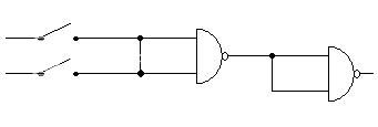
edit: this pic below was an attempt I made on richardbowles site which led me to think it might work. I used the OR gates to try and create connections that weren't (for good reason) allowed. I now realize (sort of) that this is rubbish
Solution
Both inputs connected to both inputs of a NAND gate? This sounds like a short circuit between both inputs.
After all you don't need any gate for that kind of "OR gate".
In practice connecting the inputs of a NAND results in a NOT. And having two NOTs in sequence is ID. It does nothing (only in a logical way, you can use this construct for different things in reality).
The problem is, that the OP's train of thought is only working with the switches drawn in the picture. In digital electronics you have a signal as either high (e.g. +5V) or low (GND, 0V). And you're not allowed to connect two such signals without anything between them.
OTHER TIPS
The picture you posted isn't entirely correct. It should be acting as an AND gate. This is because the second NAND gate is acting as a inverter, negating the first gate.
Because of Demorgan's theorem, an OR gate must be made with 3 NAND gates.
EDIT: Didn't see the connection between them. Yes that will act exactly like an OR gate. Interesting find.
Say the two inputs are A and B. When input A is high, the input of the NAND will be both high, so the output of the first NAND will be low. The second NAND inverts that so it will be high.
The same is true if B is high, or if they are both high. It will return low if both inputs are low.
DOUBLE EDIT: However, if the voltages are say A = 5V and B = Ground, A will flow right into the ground. This is why the standard approach using Demorgan's theorem is used.
It sounds as though you are describing the construction of an AND gate. Edit: I can see your diagram now and cannot see what is going on there. Have you actually built this circuit?
There are four basic patterns:
- Don't invert the inputs or outputs (O = A NAND B.) Result: A NAND B
- Invert only the outputs (C = A NAND B; O = C NAND C.) Result: A AND B
- Invert only the inputs (C = A NAND A; D = B NAND B; O = C NAND D.) Result: A OR B
- Invert both inputs and outputs (C = A NAND A; D = B NAND B; E = C NAND D; O = E NAND E.) Result: A NOR B
With this design, you wouldn't need any NANDs at all. But you can't connect two input signals directly in this kind of abstraction (basically, you are saying I1==I2, which doesn't make any sense). In electronics, this would result in a short circuit
The OPs solution works as long as the circuits have open collector inputs (or whatever the equivalent is called in MOS technology. open drain?) and are made to require a pull-down resistor.
However, if this is the case you don't need any gates at all, just connect the outputs together.
